VR5510 Multi-Output PMIC with SMPS and LDO
Author: EIS Release Date: Mar 28, 2021
NXP's LDO features a high-speed I2C interface (3.4 MHz) with CRC
 NXP's VR5510 is an automotive multi-output power management integrated circuit with a focus on Gateway, ADAS, V2X, and infotainment applications. It includes multiple high-efficiency switch-mode and linear voltage regulators. It offers external frequency synchronization input and output for optimized system EMC performance.
The VR5510 includes enhanced safety features with fail-safe output, becoming a full part of a safety-oriented system partitioning that covers both ASIL B and ASIL D safety integrity levels. It is developed in compliance with the ISO26262 standard. The device could also be configured to operate as a non-safety QM version part.
The device is developed and qualified in compliance with AEC-Q100 rev H (grade1, MSL3).
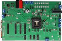
The VR5510 boards provide access to all output voltage rails as well as control and signal pins through power strip connectors. A single connector for the input power supply allows the user to supply the board with an external DC power supply to fully evaluate the performance of the device.
The evaluation board for VR5510 provides the capability to power up from the OTP fuses or in a debug mode. In debug mode, the board and GUI provide the ability to evaluate any number of configurations via the test-mode operation and the scripts generated by NXP’s GUI OTP configuration tool.
- Power management features
- One high-voltage buck converter
- Three high-efficiency, low-voltage buck converters
- Two low-voltage linear regulators with load switch option
- One medium-voltage linear regulator
- One high-voltage linear regulator with load switch option
- Directly connected to a battery
- Two low-power modes: standby and deep sleep
- System and device features
- One-time programmable (OTP) memory for flexible device configuration
- High-speed I2C interface (3.4 MHz) with CRC
- Proven and robust solution co-developed with a processor, BSP, and reference designs provided
- External clock synchronization
- Frequency spread spectrum, frequency tuning, and multi-phase operation
- Safety features
- Safety scalable: QM, ASILB, and ASILD
- Independent monitoring circuitry and dedicated interface for processor monitoring
- Simple and challenger watchdog
- PGOOD, RSTB, and FS0B safety outputs
- I2C CRC protection mechanism
- Analog built-in self-test (ABIST) and logical built-in self-test (LBIST)
- Gateways
- Mid to high infotainment/eCockpit
- Entry infotainment/connected radios
- Front-view cameras
- Surround-view
- V2X communications
- ADAS
